Water level controller circuit.
Description.
A simple but very reliable and effective water level controller circuit diagram is shown here. The circuit uses 6 transistors, 1 NE555 timer IC, a relay and few passive components. The circuit is completely automatic which starts the pump motor when the water level in the over head tank goes below a preset level and switchess OFF the pump when the water level in the over head tank goes above the full level.
Probe D is positioned at the bottom level of the tank while probes A, B and C are placed at full, half and medium levels of the tank respectively. The level sensing part of the circuit is built around transistors Q1, Q2 and Q3. When water level is below the quarter level probes A, B and C are open and the transistor Q1, Q2 and Q3 remains OFF. When the water level rises and touches the probes the corresponding transistors gets biased and switches ON. Resistors R1, R2, R3 limit the bases current of corresponding transistors while resistors R4, R5, R6 limit their collector current. LEDs D1, D2 and D3 provide a visible indication of the current water level.
When the water level goes below medium, transistor Q2 gets switches OFF and its collector goes positive. Collector of Q2 is connected to the base of transistor Q6 and as result transistor Q6 gets switched ON. Transistor Q5 will be also ON because its base in connected to the collector of Q4 which is presently OFF. As a result when the water level goes below medium relay K1 gets energised and the pump is driven. The relay is wired in the latching mode so that even if the water level goes above medium level the pump remains ON so that the tank gets completely filled. For wiring the relay in latching mode one set of N/O contacts is used. When relay is activated these contacs close which forms a short across collector and emitter of Q6. This makes the state of Q6 irrelevant to the opertion of the relay and the relay remains ON as long as the transistor Q5 is ON. The only way to make the relay OFF is by switching OFF Q5 and it is done automatically when the water level reaches the full level.
Collector of transistor Q1 is connected to the trigger pin (pin2) of IC1. When the water level reaches full level the transistor Q1 gets switched ON. As a result its collector goes to ground level which triggers the IC1 which is wired as a monostable. The output of IC1 goes high for about 1S. This makes the transistor Q4 ON for the same time and transistor Q5 whose base is connected to the collector of Q4 is switched OFF cutting the supply to the relay. This makes the motor OFF and it remains OFF until the water level again goes below the medium level.
Resistor R8 is a pull up resistor for the trigger pin of the NE555. Capacitor C3 couples the collector of Q1 to the trigger pin of NE55 and facilitates edge triggering whenever the transistor Q1 goes ON. A monostable circuit can be made edge triggered by connecting the trigger signal to the trigger input pin through a capacitor. The capacitor blocks DC and passes sudden changes. The circuit used here is termed as negative edge triggered because the monostable is triggered when ever the trigger input signal falls. R10 and R12 limits the collector current of Q4 and Q5 respectively while R9 and R11 limits their base current. R13 limits the base current of Q6 while D4 is a freewheeling diode which protects the switching transistors from voltage transients.
Circuit diagram.

Water level controller circuit diagram

Probe arrangement diagram
The probes can be arranged as shown in the diagram above. Insulated Aluminium wires can be used as the probes. The probes can be binded on a plastic rod and should be erected vertically inside the tank. The length of the probes wires and the supporting plastic rod must be chosen according to the depth of the tank. Since DC is used in the level sensing section electrolysis will occur in the probes and so the probes require small maintinances in 1 or 2 month intervals. Using AC in the sensing section will completely eliminates the chance of electrolysis and I am presently working on such a circuit. You can expect it soon.
Notes.
- Use 12V DC for powering the water level controller circuit.
- The relay I used was a 5V/220 ohm relay and that’s why the current limits resistor R12 was added in the circuit. If you use a 12V relay then the R12 can be shorted.
- Do not use a relay that consumes 500mA. Maximum collector current PN2222 can handle is 600mA.
- Use insulated single strand aluminium wires for probe and they can be arranged in the tank as per the probe arrangement diagram.
- Use a holder for mounting NE555.
- The circuit can be assembled on a Perf board.
- K1 must be a double pole relay.
- The load current, voltage ratings of the relay must be selected according to the ratings of the pump motor.
- The type number of the transistors used here are not very critical and you can do suitable replacements if any type number is not availble.
- Most of the components required for this project can be found inside your scrap box.
Power supply for this circuit.

12V DC power supply

 Notes.
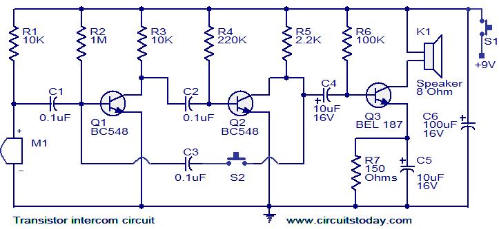


 How to make a Rheostat


