Introduction to IGBT-Insulated Gate Bipolar Transistors
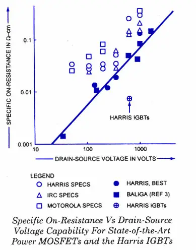
Insulated gate bipolar transistor (IGBT) is a new high conductance MOS gate-controlled power switch. The fabrication process is similar to that of an N-channel power MOSFET but employs an N-epitaxial layer grown on a P+ substrate. In operation the epitaxial region is conductivity modulated (by excess holes and electrons) thereby eliminating a major component of the on-resistance. For example, on-resistance values have been reduced by a factor of about 10 compared with those of conventional N-channel power MOSFET of comparable size and voltage capability.
Vertical MOSFETs have become increasing important in discrete power device applications due primarily to their high input impedance, rapid switching times, and low resistance. However, the on-resistance of such devices increases with increasing drain-source voltage capability, thereby limiting the practical value of power MOSFETs to applications below a few hundred volts. Here we will describe the fabrication and characteristics of a new vertical power MOSFET structure that provides an on-resistance value about one-tenth of that of conventional power MOSFETs of the same size and voltage capability. In this semiconductor device, the conductivity of the epitaxial drain region of a conventional MOSFET is dramatically increased (modulated) by injected carriers, this mechanism results in a significant reduction in the device on-resistance and leads to the acronym IGBTs.
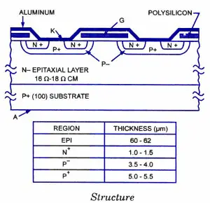
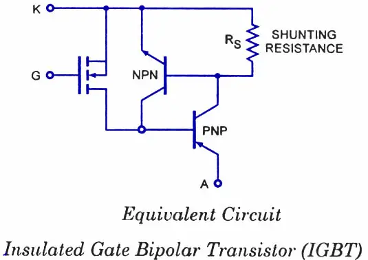
This device, while similar in structure to the MOS-gated thyristor, is different in a fundamental way; it maintains gate control (does not latch) over a wide range of anode current and voltage. The structure and the equivalent circuit of the IGBT and IGBT schematics is shown in figures respectively. They are similar to those of an MOS-gated thyristor, except for the presence of the shunting resistance RG in each unit cell. The fabrication is like that of a standard N-channel power MOSFET except that the N~ epitaxial silicon layer is grown on a P+ substrate instead of an N+ substrate. The heavily doped P+ region in the center of each unit cell, combined with the sintered aluminium contact shorting the N+ and P+ regions, provides the shunting resistance RS shown in IGBT schematics figure.This has the effect of lowering the current gain of the N-P-N transistor (αN-P-N) so that αN-P-N + αP-N-P < 1- Thus latching is avoided and gate control is maintained within a large operating range of anode voltage and current.
How IGBT works ? (IGBT Operation)
The IGBT is a four layer N-P-N-P device with an MOS-gated channel connecting the two N-type regions. In the normal mode of operation of an IGBT, a positive voltage is applied to the. anode (A) relative to cathode (K). When the gate (G) is at zero potential with respect to K, no anode current IA flows for anode voltage VA below the breakdown level VBF. When VA < VBF and the gate voltage exceeds the threshold value VGT, electrons pass into the N~-region (base of the P-N-P transistor). These electrons lower the potential of the N~-region, forward biasing the P+-N~ (substrate-epi-layer) junction, thereby causing holes to be injected from the P+ substrate into the N- epi-layer region. The excess electrons and holes modulate the conductivity of the high resistivity N-region, which dramatically reduces the on-resistance of the device. During normal operation, the shunting, resistor Rg keeps the emitter current of the N-P-N transistor very low, which keeps αN-P-N very low. However, for sufficiently large emitter current IA significant emitter injection may occur in the N-P-N transistor, causing αN-P-N to increase; in this case the four-layer device may latch, accompanied by loss of control by the MOS gate. In this event, the device may be turned off by lowering emitter current IA below some holding value, as is typical of a thyristor. This explains how igbt works and its mode of operation.
IGBT Characteristics and IGBT specification.
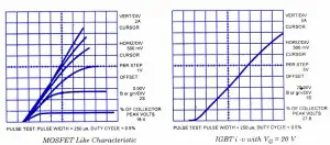
With zero gate bias, the forward characteristic of a IGBT shows very low current (< 1 nA) up to 390 V, where it breaks-up sharply to much larger current levels with only a slight increase in voltage. If the internal junction between the P+ substrate and the N~ epitaxial layer had been edge passivated, a similar reverse breakdown characteristic would be expected. The actual reverse breakdownvoltage of the device would be about 100 V if edge passivation is not used.
Igbt schematics (characteristic ) shows the MOSFET like transfer characteristics of an IGBT in the low voltage region. A noteworthy feature of the IGBT characteristics is the – 0.7 V offset, from the origin, of the steeply rising portion of the i-v characteristics. This offset is the voltage required to forward bias the P+-N~ (substrate-epi-layer) junction. range 10-30 A in 3 mm square chips. The magnitude of latching current has been found to depend on both anode voltage and temperature, decreasing with increasing anode voltage or increasing temperature
IGBT latching current
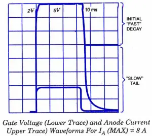
More interestingly, the latching current is also strongly influenced by the gate voltage turn-off time. Slow gate turn-off (- 10 us) permits anode currents upto 30 A without latching. However, rapid gate turn- off (< 1 us) leads to latching at a much lower anode current level (- 10 A) in the same device. It is believed that latching during rapid turn-off of the gate voltage is due to current being forced through the N-P-N transistor causing αN-P-N to increase, and leading to the condition for latching, αN-P-N + αP-N-P= 1. Slow turn-off of the gate voltage prevents this, since the induced channel turns off slowly and partially shunts the N-P-N transistor; the small current through this transistor keeps αN-P-N sufficiently low to avoid IGBT latching.
Improved IGBTs with fast switching speed and high current capability are available from Harris Semiconductor. The modified structure is shown in figure.. It differs from that in other IGBT schematic by the addition of a thin (- 1.0 mm) layer of N+ silicon in the epitaxial structure between the N-region and the P+ substrate. This N+ layer lowers the emitter injection efficiency of the P-N-P transistor in the equivalent circuit, and results in an increase in IL by a factor of 2 to 3. In addition, there is also a reduction in tF
Share this on your favourite network



Hi! Thanks for sharing your article about IGBT...
ReplyDelete